Breakthrough in photonic chips: cheap production through nanoprinting
The Chinese semiconductor start-up Prinano has reported a possible breakthrough in the production of photonic chips: it has succeeded in producing them in a production-related environment and significantly reducing the necessary costs.
Avoid expensive lithography systems
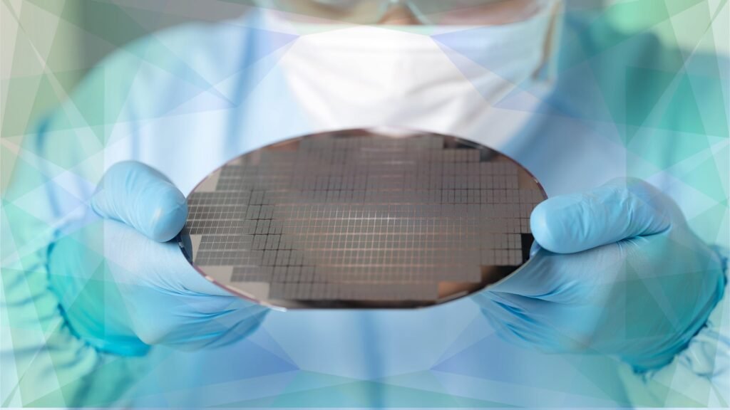
The company said it produced 8-inch optical semiconductor wafers without the need for industry-standard DUV lithography systems, the company reported South China Morning Post. The development could strengthen China’s efforts to reduce its dependence on key Western technology. As Prinano announced, the wafers were created together with the company Shenzhen Litra Technology. Instead of the usual projection of circuit structures using ultraviolet radiation, the process relies on nanoimprint lithography. Microscopically small structures are embossed directly into a specially prepared coating on the wafer. This means that expensive optical components, such as those used in modern DUV or EUV systems, are largely unnecessary.
According to the company, its own PL-AS technology is intended to reduce production costs to around a tenth of conventional DUV processes. In addition, structures with a size of less than ten nanometers are possible. Prinano sees this as an important step towards the industrial use of the technology. Nanoimprint lithography has been considered a promising alternative to classic chip production for years.
To date, however, widespread introduction has often failed due to problems such as defects, wear of the embossing stencils, limited production speeds and fluctuating yields. Prinano has been working to overcome these challenges since its founding in 2017. According to its own information, the company had already delivered China’s first domestic nanoimprint lithography system to a customer in 2025.
Independent confirmation is still pending
However, the focus is not on high-performance processors or AI accelerators, but on photonic chips. These components process light signals instead of electrical signals and are used, among other things, in fiber optic networks, data centers, sensor systems and LiDAR applications. The embossing technology is particularly suitable for such components because many of their structures consist of regularly recurring nanopatterns. The use of 8-inch wafers is also considered notable. Although the most modern processors are largely manufactured on 12-inch wafers, 8-inch formats are still widely used in specialized areas such as power electronics or compound semiconductors.
Successful wafer-level manufacturing therefore indicates a step beyond pure laboratory testing. However, it remains unclear how economical the process actually is. Prinano did not publish information on production volumes and yields or independent confirmation of the results. Whether the technology is commercially competitive remains to be seen.
Research Snipers is currently covering all technology news including Google, Apple, Android, Xiaomi, Huawei, Samsung News, and More. Research Snipers has decade of experience in breaking technology news, covering latest trends in tech news, and recent developments.