Samsung Starts Mass Production of 14nm DRAM to Stay Ahead of Competition
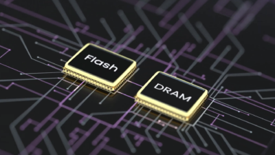
Samsung has started mass production of 14nm DRAM chips and aims at becoming a leader in the global memory chip business.

Samsung has announced the mass production of 14nm DRAM chips using the EUV (Extreme Ultraviolet) technology. This technology reduces power consumption, improves performance, and reduces development time.
The company used EUV to five layers of DDR5 DRAM. This improves productivity per wafer and power consumption by 20% compared to previous-generation chips. The company launched its first DDR5 DRAM sticks with eight layers of 16GB chips, resulting in a total capacity of 512GB in March this year. For these newer 14 nm DDR5 DRAM modules, the company will use eight layers of 24Gb chips.
Initially, these chips will be used in cloud servers and data centres for AI, Big Data, and ML processes.
Senior vice president and head of DRAM Product & Technology at Samsung Electronics, Jooyoung Lee, said,
We have led the DRAM market for nearly three decades by pioneering key patterning technology innovations. Today, Samsung is setting another technology milestone with multi-layer EUV that has enabled extreme miniaturization at 14nm — a feat not possible with the conventional argon fluoride (ArF) process. Building on this advancement, we will continue to provide the most differentiated memory solutions by fully addressing the need for greater performance and capacity in the data-driven world of 5G, AI and the metaverse.
With the best manufacturing process and highest performance, Samsung aims at becoming a leader in the global memory chip business.
Alexia is the author at Research Snipers covering all technology news including Google, Apple, Android, Xiaomi, Huawei, Samsung News, and More.


