The importance of Signal Integrity and Thermal Management in high-speed PCB design
With the increasing speed, size reduction and density of electronic devices, printed circuit board (PCB) design has become a balancing act between electrical performance, heat dissipation and physical constraints. A board that performs well at low frequencies can behave quite differently when handling high-speed signals. At these speeds, even minor design choices such as trace geometry, material selection, component placement, and thermal pathways can impact the performance of the entire system.
Signal integrity and thermal management are two key considerations. They are often considered as distinct engineering problems, but they are closely related. Low signal strength can affect data transfer, and high temperatures can alter electrical properties, shorten component life, and decrease system reliability. For modern high-speed electronics, it is important to design for both from the outset.
Maintaining signal integrity is a challenge
Signal integrity refers to the fidelity of an electrical signal as it moves from its source to its destination. A PCB trace is not just a passive link between two components in high-speed circuits. It acts like a transmission line, and the propagation of the signal is affected by the impedance and the electromagnetic environment of the line.
If these effects are not taken into account in the design of a board, engineers can experience reflections, ringing, crosstalk, electromagnetic interference, and timing errors. These issues can be particularly important in interfaces with high data rates, fast switching edges, differential pairs, memory buses, and high frequency communication circuits.
There are a number of design practices that help control these risks:
Impedance control: Trace width, copper thickness, dielectric properties and distance between signal and reference planes all affect impedance. Keeping the necessary impedance reduces reflections.
Careful routing: Short, straight routes, spacing and well controlled layer transitions can minimize unwanted coupling and discontinuities.
- Reliable reference planes: Continuous ground or reference planes offer predictable return current paths. Splits, gaps, and misplaced vias can cause current to flow on less desirable paths.
- Stack-up planning: Choosing the layer stack-up and dielectrics early allows engineers to plan for controlled-impedance routing and control electromagnetic coupling.
Termination and via management: Proper termination can minimize reflections, and unnecessary vias and poorly designed transitions can create parasitic effects.
The role of simulation and measurement is also important. Signal-integrity analysis can be used to detect impedance discontinuities and coupling issues prior to manufacturing, and testing can be used to verify that the assembled board meets expectations.
Why Thermal Management is more than Heat Removal
High-speed PCBs may include processors, power-management devices, memory, radio-frequency components, and other components that produce significant heat in a small area. With the density of components, there are fewer opportunities for heat to escape, and thermal design is a critical aspect of the electrical design.
High temperature can lead to leakage current, change the characteristics of components, narrow the operating margin, and shorten the service life. The PCB can also experience mechanical stress due to the difference in thermal expansion between copper, laminate, solder, and components as a result of temperature changes.
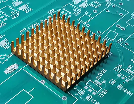
Thermal management is thus more than just attaching a heatsink to a board after it has been laid out. It involves knowing where the heat is coming from, how it is flowing through the board, and where it can be safely dissipated.
These problems are typically solved by component placement, copper plane design, thermal vias, selection of the right laminate, airflow planning, and heatsinks or other cooling solutions as needed. Thermal simulations can be used to identify hotspots and to compare design options prior to prototype construction.
It depends on the application which is the right approach. The thermal requirements of a compact networking device, an industrial controller, and a high-performance computing board can be quite different. In both instances, cooling decisions need to be considered in conjunction with electrical performance, mechanical constraints, manufacturing cost, and space.
The relationship between Signal Integrity and Heat
Signal integrity and thermal management are coupled as electrical behaviour affects temperature and vice versa. The resistance to copper increases with temperature, which may impact voltage drop and power loss. Other operating characteristics of semiconductor devices can also be temperature dependent, such as timing and leakage. These changes can cause a loss of signal margins or less predictable performance in sensitive designs.
Another point of connection is power delivery. Transient current demands can cause voltage fluctuations in the power distribution network, and high-speed components need stable power and ground networks. Poor power integrity can manifest itself as noise in sensitive circuits or as intermittent system failures. In the meantime, power-delivery paths have resistive losses that produce heat, which can result in local hot spots.
Trade-offs can also occur in layout decisions. A designer might want to put components near each other to keep high-speed signal paths short, but high power consumption can make cooling more challenging. On the other hand, splitting up components to enhance thermal conditions can increase signal routes or make routing more difficult. The goal is not to optimize each issue separately, but to determine a layout that meets both electrical and thermal needs.
This is why it is important to have a coordinated workflow for high-speed PCB development, where electrical, thermal, mechanical, and manufacturing considerations are all reviewed together, and not after issues have arisen.
Design Decisions that Make a Difference
A good design process starts before routing. Signal speeds, edge rates, impedance, power consumption, environmental conditions, and acceptable temperature limits should be specified early in the project by the engineers. These requirements dictate the selection of materials, stack-up, copper weight, board thickness, and component layout.
Then, simulation can be performed to evaluate critical signal paths, power distribution and thermal behaviour. While models rely on the accuracy of the data they are based on, they can reveal potential vulnerabilities and allow teams to evaluate options before they go into fabrication.
Manufacturability should always be a part of the conversation. In some cases, fine traces, dense via structures, controlled impedance and special materials can enhance performance, but they also impose fabrication limitations and cost factors. Design rules should be based on the capability of the process to be used for manufacturing, not just an idealized layout.
Prototyping and validation are still key. Impedance measurements, time domain reflectometry, eye diagram analysis, thermal imaging and temperature testing can identify problems that simulation alone may not identify. When a product needs to be reliable for extended periods of time, testing under realistic workloads and environmental conditions is particularly critical.
As part of their research into board production and manufacturing considerations, engineers can also look at technical resources from PCB specialists like MCHDIPCB. The key is to compare any supplier’s documented capabilities and process controls to the specific requirements of the design, and not assume that a specific manufacturing option will automatically solve signal-integrity or thermal issues.
Designing for reliability
When it comes to high-speed PCB performance, it is not just about one feature. A good laminate will not make up for poor routing, and a good routing will not make up for a poor power-delivery network or uncontrolled component temperatures. Reliability becomes a reality when the electrical, thermal, mechanical and manufacturing needs of the board are considered as part of the same engineering problem.
With the increasing data rates and shrinking electronic products, the early involvement of layout engineers, signal-integrity engineers, thermal engineers, and manufacturing engineers is more valuable. It can minimize late stage redesigns, increase the chances of prototypes achieving their goals, and ensure consistent performance in the field.
In the end, signal integrity ensures that the information flowing through a circuit is of high quality and on time, while thermal management ensures that the circuit operates at a stable temperature over time. In high-speed PCB design, neither is an optional refinement. Both are essential to creating electronics that will function well under heavy workloads.

Alexia is the author at Research Snipers covering all technology news including Google, Apple, Android, Xiaomi, Huawei, Samsung News, and More.