IBM: This is how chips shrink below the 1 nanometer limit
The US technology group IBM has presented a new approach that aims to enable the construction of ever smaller semiconductor products with ever higher transistor densities. Ultimately, this should make chips with a structure width of less than one nanometer possible.
IBM wants to increase transistor density with a new approach
Moore’s Law has been increasingly reaching its limits in recent years; after all, more and more effort has to be made to further shrink the structure widths of modern chips. IBM has now presented its variant of a possible solution in which the transistor density in new chips can be further increased in order to ultimately achieve calculated structure widths of just 0.1 nanometers. The US group has developed a manufacturing technology with which it is currently able to achieve chips with a structure width of just 0.7 nanometers or 7 angstroms (7A), if one uses the current standards for the so-called nodes of chip production.

Transistors on multiple floors, not just stacked wafers
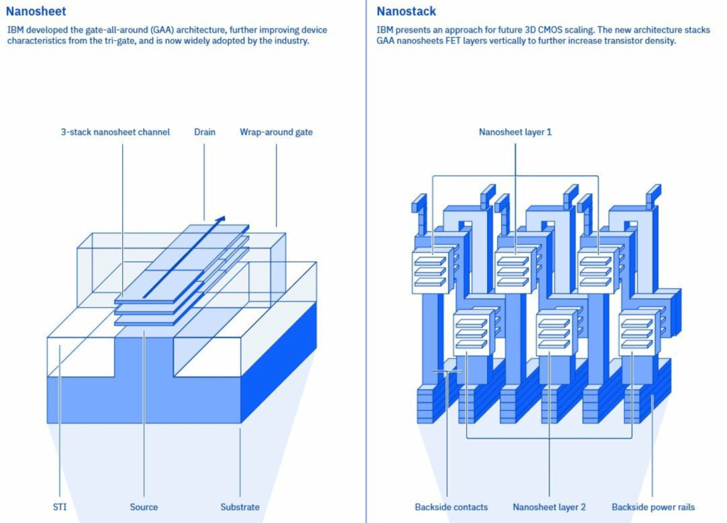
IBM says it wants to rely on so-called nanostacks and arrange transistors on top of each other in several levels. Several so-called nanosheets – i.e. layers of transistors – are positioned in a slightly offset “stacked” manner, thus achieving a significant increase in transistor density while maintaining the same base area. In this way, the need to further reduce the structure width on a horizontal level is overcome.
According to IBM, new technologies have been developed with which the front and back of the staggered transistors on the different levels can be supplied with signals and energy separately. It is said that through so-called single dieelectric bonding, the transistors can be optimized independently at different levels.
50 percent more performance compared to 2nm
According to IBM, the newly developed nanostack technology can be used in CPUs, GPUs or even memory products. The result should be up to 50 percent increased performance or up to 70 percent improved efficiency compared to current 2-nanometer chips. In all of this, it is important to remember that IBM has not found a way to shrink the horizontal distances between the transistors and other structures in a chip. Essentially, they are adapting an approach that has been followed by TSMC, Intel and other chip manufacturers for several years. You build higher instead of reducing the distance on the surface. Unlike TSMC & Co, IBM does not simply rely on stacking several wafer layers in the form of nanosheets, but instead wants to arrange its transistors in several levels within these so-called nanosheets.
IBM itself has also been using nanosheets for some time to achieve higher transistor densities. It will be some time before IBM uses its nanostack technology in the first chips. IBM says it will take around five years for the approach to lead to chips with a theoretical structure width of 0.7 nanometers. Since the company itself is no longer active as a chip manufacturer, third-party companies can license the technology and use it in partnership with IBM. So far this has been the case, for example, with the Japanese manufacturer Rapidus or Samsung.
Research Snipers is currently covering all technology news including Google, Apple, Android, Xiaomi, Huawei, Samsung News, and More. Research Snipers has decade of experience in breaking technology news, covering latest trends in tech news, and recent developments.